Site Map
|
English
/
繁中
/
简中
Company Profile
Quality Policy Statement
GCS History
Business Contact
Technology
Overview
GaAs & GaN RF Technologies
InGaP HBT
High Linearity InGaP HBT
High Voltage and GSM InGaP HBT
VCO InGaP HBT
Super High ƒmax HBT
GaAs pHEMT
0.5um D-Mode T-Gate pHEMT
0.5um Switch pHEMT
0.25um E/D-Mode LN pHEMT
0.25um D-Mode T-Gate pHEMT Power Process
0.15um Low-Noise & Power pHEMTs
HFET
GaN/SiC HEMT
Integrated Passive Devices
THz Schottky Diode
Varactor Diode
InP HBT Technologies
GaN/SiC HEMT Technologies
BAW Technologies
Optoelectronics Technologies
Foundry Services
GaAs & GaN RF Wafer Foundry
InP HBT Wafer Foundry
OPTOELECTRONICS Wafer Foundry
Customer Proprietary Process Manufacturing
Manufacturing Capabilities
Processing Capabilities
Testing Capabilities
Foundry Support
Foundry Support Flow
MPW Support
Process Design Kit
CAD Tools and Support
Testing Services
Foundry Training
Foundry Partners
GaAs & InGaAs PIN Photodetectors & Arrays
APD
VCSEL Chips & Arrays
Sales Rep
Financials
Monthly Sales
Quarterly Sales
Financial Reports
Annual Reports
Shareholder Services
Stock Quote
Contact
Investor Conference
TSE Market Observation Post System (MOPS)
Corporate Governance
Board of Directors
Audit and Compensation Committee
Pure-play Wafer Foundry
Pure-play Wafer Foundry
Technology
Foundry Services
GaAs & GaN RF Wafer Foundry
InP HBT Wafer Foundry
OPTOELECTRONICS Wafer Foundry
Customer Proprietary Process Manufacturing
Manufacturing Capabilities
Processing Capabilities
Testing Capabilities
Foundry Support
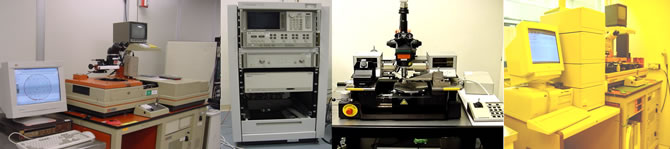
Home > Pure-play Wafer Foundry > Foundry Services > Manufacturing Capabilities > Testing Capabilities
Testing Capabilities
100% on-wafer Automated DC and RF Testing
DC (die sorting)
RF (up to 20 GHz): OIP3, harmonics, Oscillator, S-parameters, etc.
Engineering Characterization Support (Up to 40 GHz)
Device Modeling (linear and non-linear models)
DC parametric test
RF small signal/large signal characterizations (load pull, OIP3, noise parameters etc.)
Automatic Wafer Mapping With Ink or Inkless Electronic Wafer Mapping